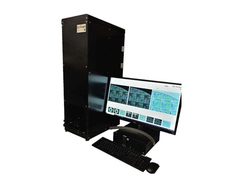
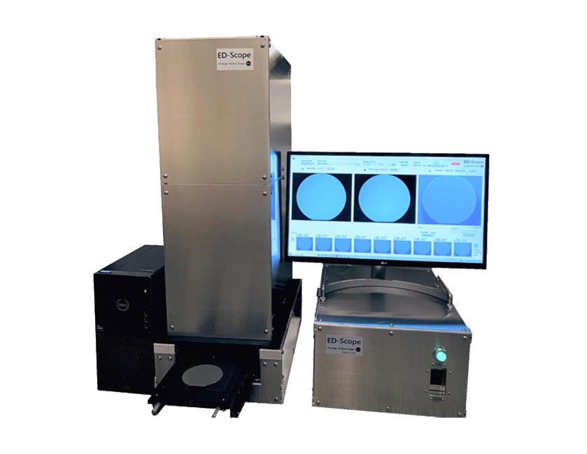
We are honored to introduce to you the ED-Scope series of surface/internal defect detection devices (ED machines), mainly used for various transparent or opaque semiconductor wafer defect detection.
Based on independent optical technology, lighting technology, and image processing technology, ED machines can clearly visualize normally difficult to confirm defects using images, and can see defects that cannot be seen under general inspection in a broader field of view.
The depth Z direction can reach the nanometer level, and the detection results can be observed macroscopically to quickly detect/confirm nano defects in the tested object.
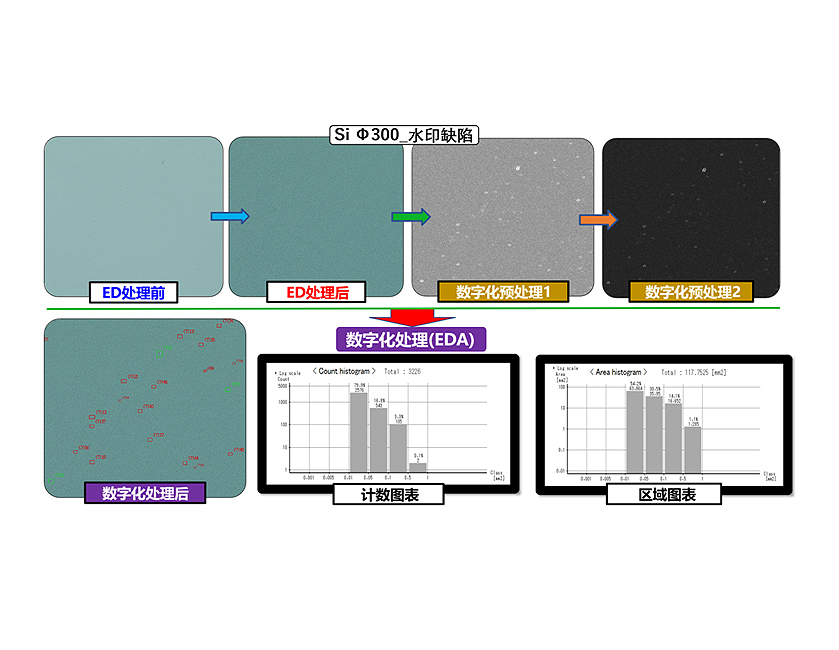
Semiconductor, compound semiconductor (Si, SiC, GaAs, Ga2O3, InP, GaN, LiTaO3, etc.),Semiconductor processing products (bonded wafers, deposited wafers, wafer lithography, etc.),Defects (scratches, cracks, dents, watermarks, cutting marks, slip lines, cavities, foreign objects, etc.) on the wafer surface facial mask or substrate can be visually inspected and evaluated with the LCD through ED technology.And through ED technology, data such as defect location, defect size, and overall appearance of the wafer can be recorded in detail, and digital management can be conveniently carried out.It has become a highly accurate one-stop automatic analysis and inspection equipment.
Nanoscale micro grinding marks, orange peels, scratches, as well as internal micro veins, crystal defects, etc. remaining on the surface of glass, crystal, sapphire, etc,It can also be visually inspected and evaluated.The management records of surface roughness, the improvement of polishing conditions, and the improvement of finished product rate after evaporation are of great help.
In addition, by connecting the robot of the automatic handling system (optional, corresponding to the installation in the clean room), unmanned automatic analysis and detection in the factory can be achieved.
《Equipment Specifications》
● Detection method: reflective&refractive
● USB camera: 5 megapixel color
● Sensitivity adjustment function: 8 segments can be switched
● ED processing automation device (PC automatic control)
● ED processing automation software
● Field of view: Φ 136 (H) × 115 (V)~34 (H) × 28 (V) mm
● 1 field of view processing time: approximately 10 seconds
● White LED: 3W
● Equipment size: 300 (W) × 470 (D) × 900 (H) mm
★ Composite Stereoscopic Image Processing (ED Processing)
★ Defect extraction processing (EDX processing)
★ Digital processing (EDA processing)